
AMADEus Seminar - Dr. Augustin Mihi - Friday 3 April 2015, 11:00 am - CRPP
le vendredi 03 avril 2015 à 11hDr. Agustín Mihi
Universitat Rovira i Virgili Tarragona, Spain
Low Cost and Large Area Photonic Architectures for Enhanced Light Management in Optoelectronic Devices
Nanostructured dielectric and metallic photonic architectures can concentrate the electric field through resonances, increase the light optical path by strong diffraction and exhibit many other interesting optical phenomena that cannot be achieved with traditional lenses and mirrors. The use of these structures within actual devices will be most beneficial for enhanced light absorption in thin solar cells, photodetectors and to develop new sensors and light emitters. However, emerging optoelectronic devices rely on large area and low cost fabrication routes such as roll to roll or solution processing, to cut manufacturing costs and increase the production throughput. If the exciting properties exhibited photonic structures are to be implemented in these devices then, they too have to be processed in a similar fashion as the devices they intend to improve. In this presentation, I will describe different low cost and large area photonic architectures that coupled to these new types of technologies facilitate enhanced light matter interaction within the active layer and are fully compatible with current manufacturing processes.
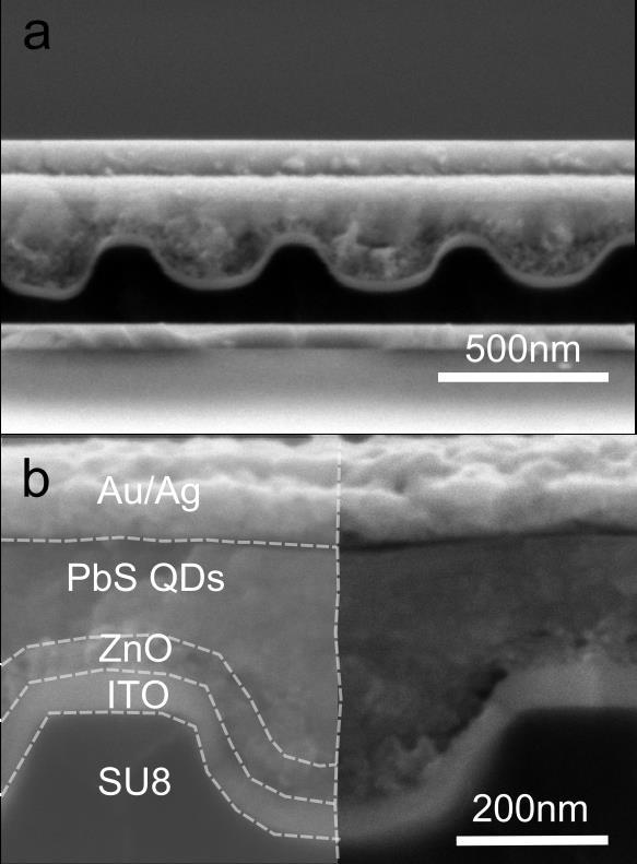
Cross-?sectional SEM image of a ZnO-?PbS solar cell built on top of an photonic electrode.